Hack & Jack
Hack is a 16-bit general-purpose computer I built with hardware simulators, based on the Von Neumann architecture. Jack is a simple programming language modeled after Java, with a compiler I wrote in C++. I built the Hack computer and the Jack compiler with implementation suggestions from 'The Elements of Computing Systems' by Nisan and Schocken, which is basically the book version of Nand2Tetris.
In summary, this project involved building out the following:
- Hack Computer → Used the Hack HDL language to build fundamental chips that could be composed together to form the ALU, CPU, n-bit registers, RAM and ROM modules for a 16-bit general-purpose computer.
- Hack Assembler → Developed an assembler using C++ that converts source code written in the Hack assembly language into machine code that is directly executable by the CPU built previously.
- Jack VM Translator → Implemented a stack-based virtual machine and VM translator using C++ that compiles source code in the Jack VM language into Hack assembly code.
- Jack Compiler → Implemented a recursive descent compiler using C++ that converts Jack source code into the Jack VM language which can then be passed through the VM translator built previously to get Hack assembly code as part of a 2-step compilation model, similar to that of Java or C#.
- Hack OS → Implemented a rudimentary and unoptimised operating system using Jack that provides abstractions for high-level programs such as I/O device interfacing, heap memory allocation/deallocation, screen graphics drawing, and so on.
The Hack Computer
Hack is a simple 16-bit general-purpose computer based on the Von Neumann architecture. It's built using chips defined with the Hack HDL language provided as part of Nand2Tetris.
I started the journey from as low of a level as possible (but skipping most of the physics and chemistry), progressing through concepts and building things out in the order below.
-
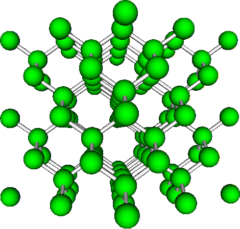
Silicon crystals and doping — impurities such as phosphorous and boron are 'injected' into pure silicon crystals to form what are called n-type semiconductors and p-type semiconductors.
-
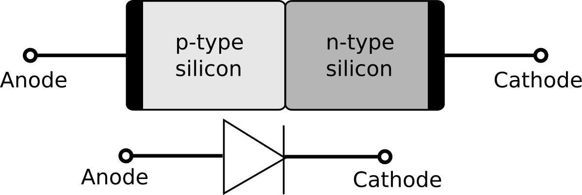
P-N junctions and diodes — an interesting result of physically joining an n-type semiconductor and p-type semiconductor is that an electric potential difference exists across the junction. This enables unidirectional current flow, letting us implement a simple diode device.
-
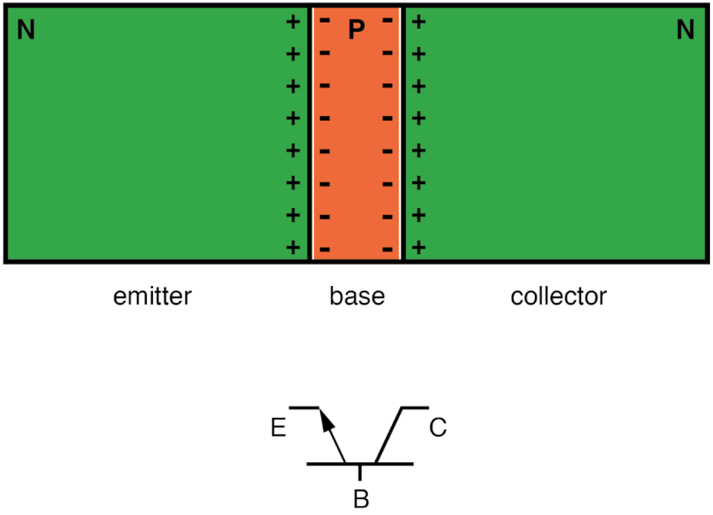
NPN/PNP transistors — simple transistor devices can be formed from physically joining n-type and p-type semiconductors in either the n-p-n configuration or p-n-p configuration.
-
Logic gate implementation using transistors and resistors — the primitive logic gates such as AND, OR and NOT can be implemented using transistors and resistors. Starting with these gates, we easily have access to other gates such as XOR, NAND, NOR, etc.
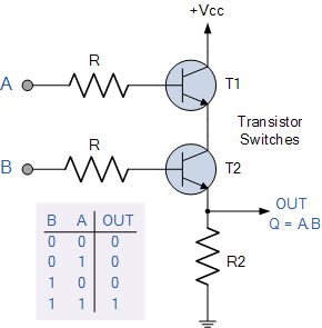
AND gate implementation. -
Logic design with primitive logic gates — it was proven in 1913 that NAND is a universal logic gate, meaning that any boolean function can be implemented solely using NAND gates. The implication is that literally all of the chips after this stage can be built entirely from just NAND gates.
AND gate implementation. -
Multiplexer and demultiplexer implementation — multiplexers take in multiple data inputs and use some control inputs to select out which input to pass through to the output. Demultiplexers take in a single input signal and direct it towards one of many output pins, using control bits.
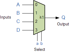
4-way mux chip. -
Adder chips (half-adder, full-adder and incrementer) — from primitive logic gates, we can construct a basic 'half adder' that adds two 1-bit numbers, which can then be composed together to form 'full adders' capable of adding three 1-bit numbers, which can then be composed together to form 16-bit adder chips, capable of adding two 16-bit numbers.
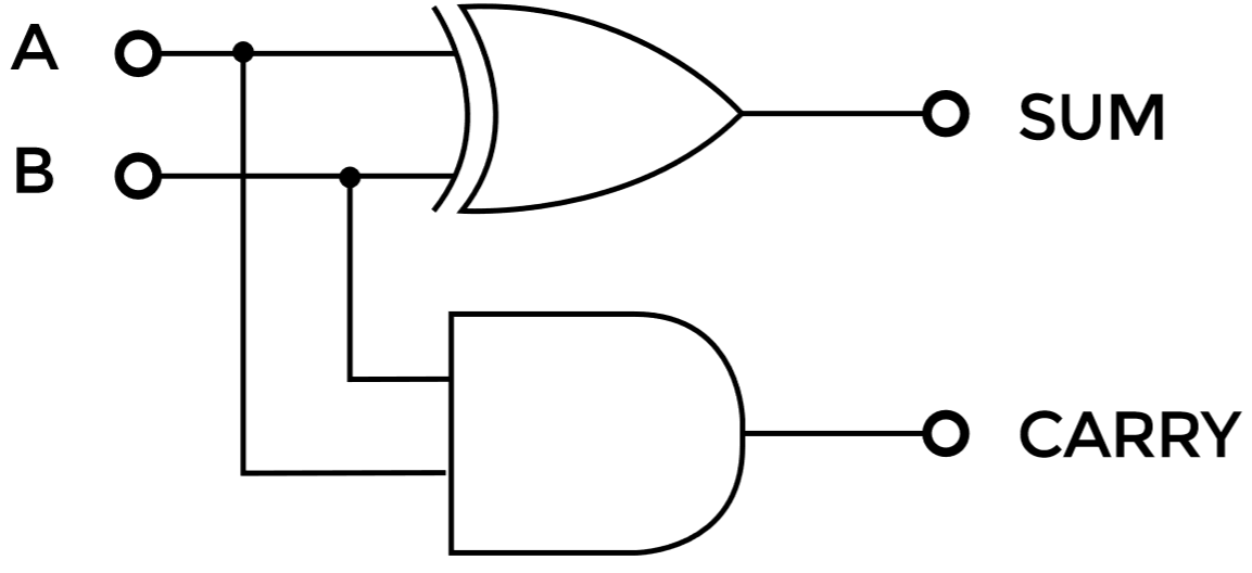
Half adder. 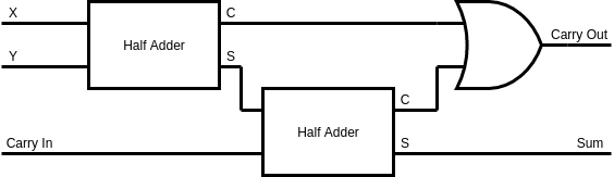
Full adder. 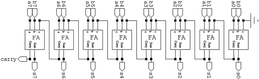
8-bit ripple carry adder chip. -
Arithmetic logic unit implementation — using a bunch of multiplexers, demultiplexers, AND gates and a 16-bit adder, you can implement a basic ALU capable of addition, subtraction and logical operations, AND, OR and NOT, on 16-bit inputs.
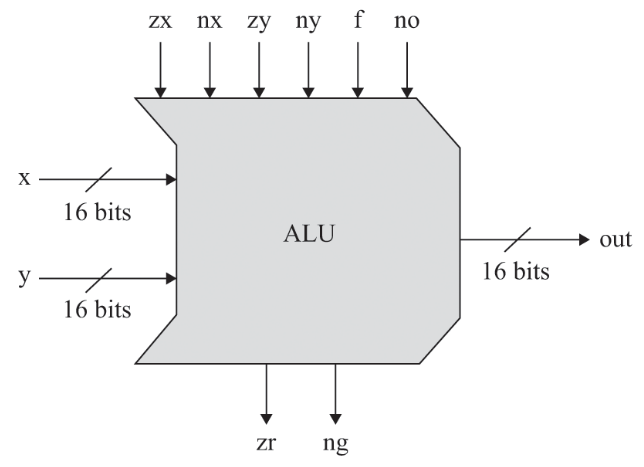
ALU chip. The inputs zx, nz, zy, ny, f, and no are control bits that determine what arithmetic-logic operation to perform. 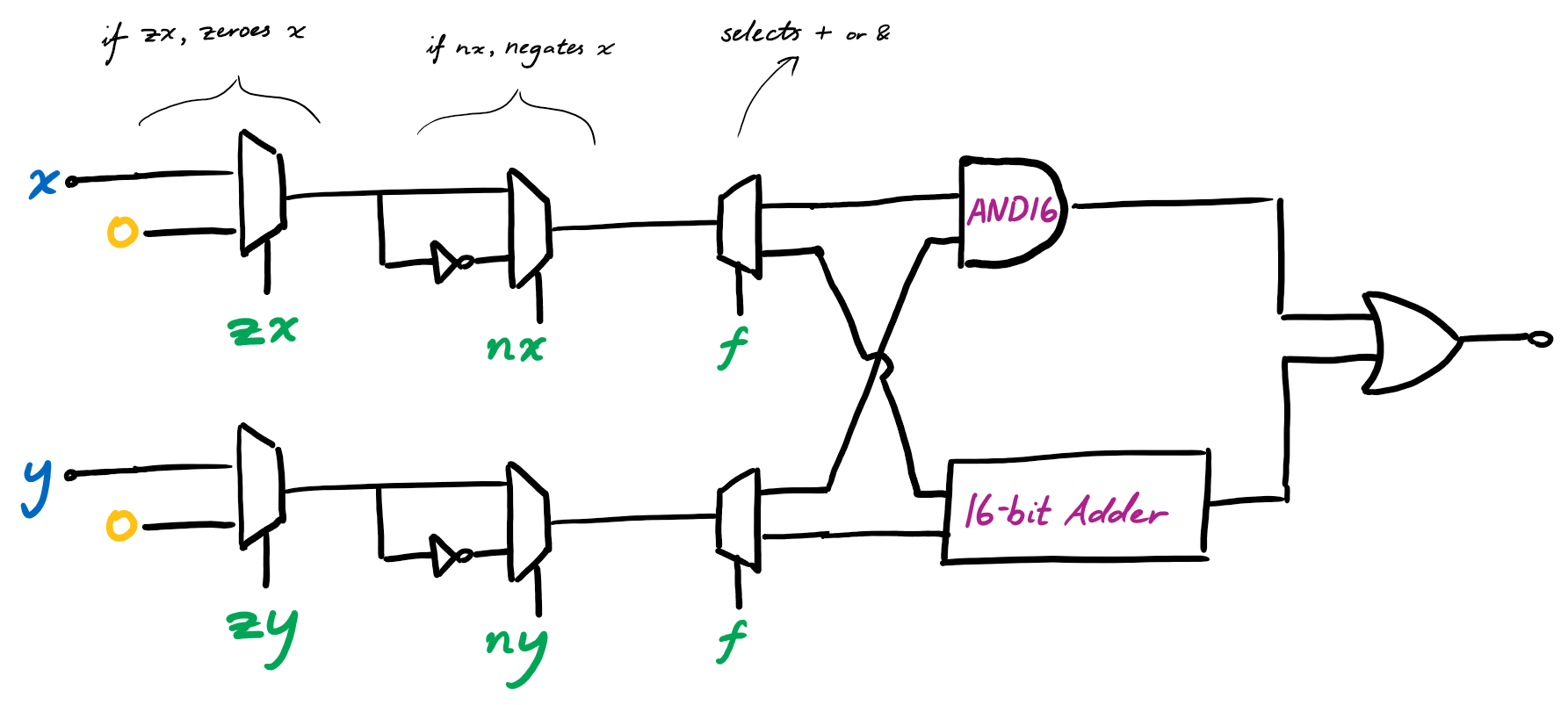
My implementation of the ALU. -
Combinational vs. sequential chips and quartz clocks — combinational chips are those whose functionality is independent of time. Sequential chips are those that depend on a concept of previous time cycles. To introduce the concept of working memory for a computing system, we need a concept of time units for the registers that will ultimately be used to construct the RAM device. This can be done with a central quartz clock, a piezoelectric material that generates signals at a very precise frequency.
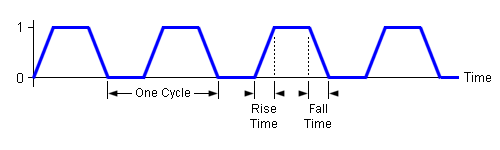
Example clock signal. -
Latches: S-R latches, data flip-flops (D latches) — latches are digital circuits that can maintain state over time. Mainly, there are S-R latches, which can be set to either an on/off state, and data flip-flops, which build on top of S-R latches, that form the fundamental units that ultimately can be composed together to form RAM chips.
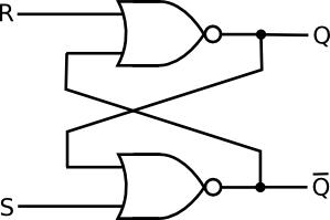
S-R latch implementation. 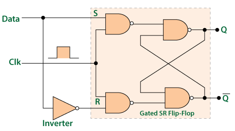
Data flip-flip implementation. -
1-bit and n-bit register construction — registers are devices that hold and emit a value. A 1-bit register, which simply holds either a 0 or a 1 and emits it as its output, can be constructed by joining a multiplexer with a data flip-flop. An 16-bit register, which can hold sixteen 0s or 1s and emit them each, can be constructed by joining, in parallel, sixteen 1-bit registers.
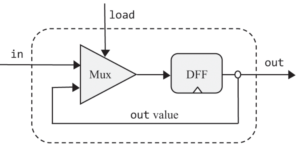
1-bit register implementation. 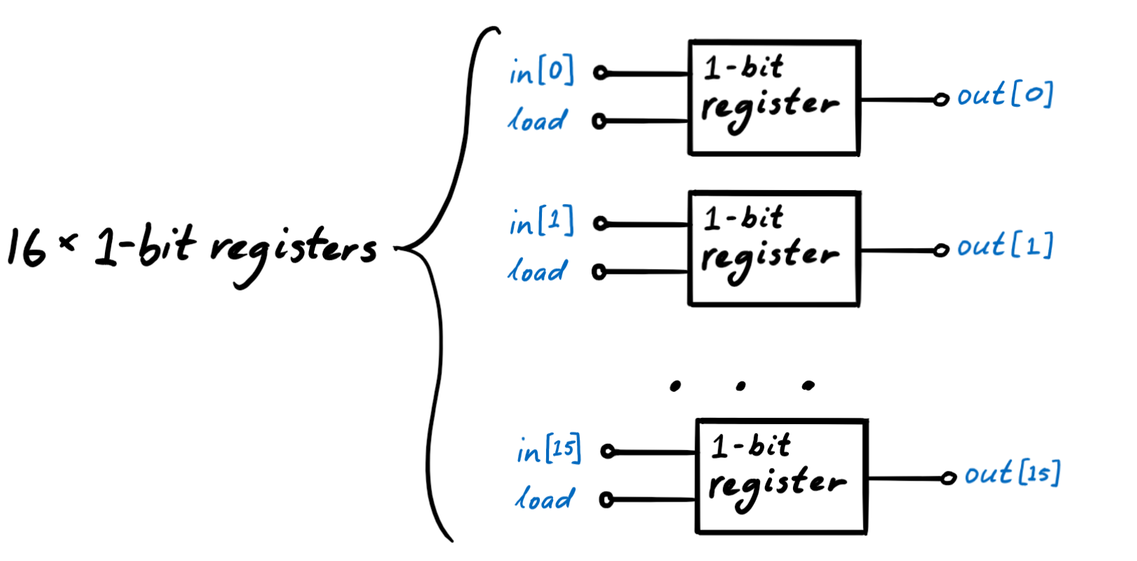
Sixteen 1-bit registers form a 16-bit register -
Recursive ascent construction of RAM modules — RAM is essentially just a big array of registers, each of which is addressable with a value in range which is what we call a memory address. By joining eight 16-bit registers in parallel, we can form a tiny RAM chip that can store eight 16-bit values. By joining eight of these RAM chips in parallel in the same fashion, we can create a bigger RAM chip with eight times the memory capacity. This recursive construction can be repeated endlessly.
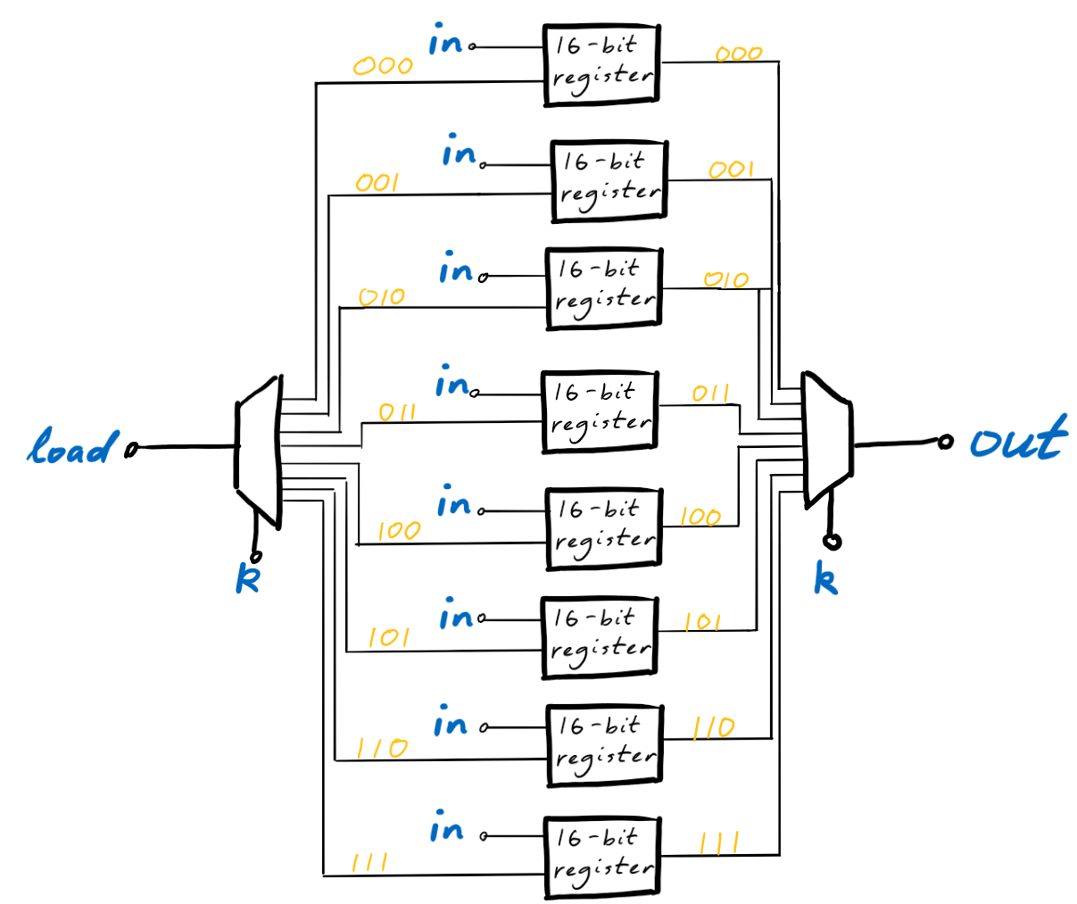
RAM8 chip. 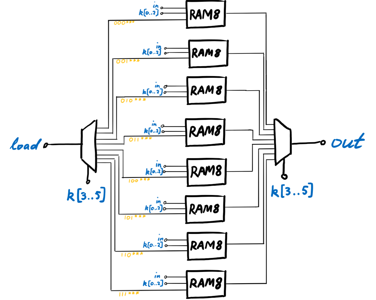
RAM64 chip, constructed using RAM8 chips. -
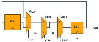
Counter chip implementation (for the program counter register) — there's usually a dedicated register called a counter aboard the CPU that has an interface for loading a new value, reseting the value, and incrementing the current value. This dedicated chip is the program counter register. It can be assembled using an incrementer chip (built alongside the adder chips previously), multiplexers, and a 16-bit register.
Counter chip implementation. -
Computer architecture: defining the Hack instruction set and assembly language — the instruction set for the Hack machine is very compact, consisting of only 2 instruction types:
- Addressing instructions called A-instructions, which read a value into a dedicated address register called the 'A register'.
- Computation instructions called C-instructions, which executes an arithmetic-logic hardware operation and stores the result in some register.
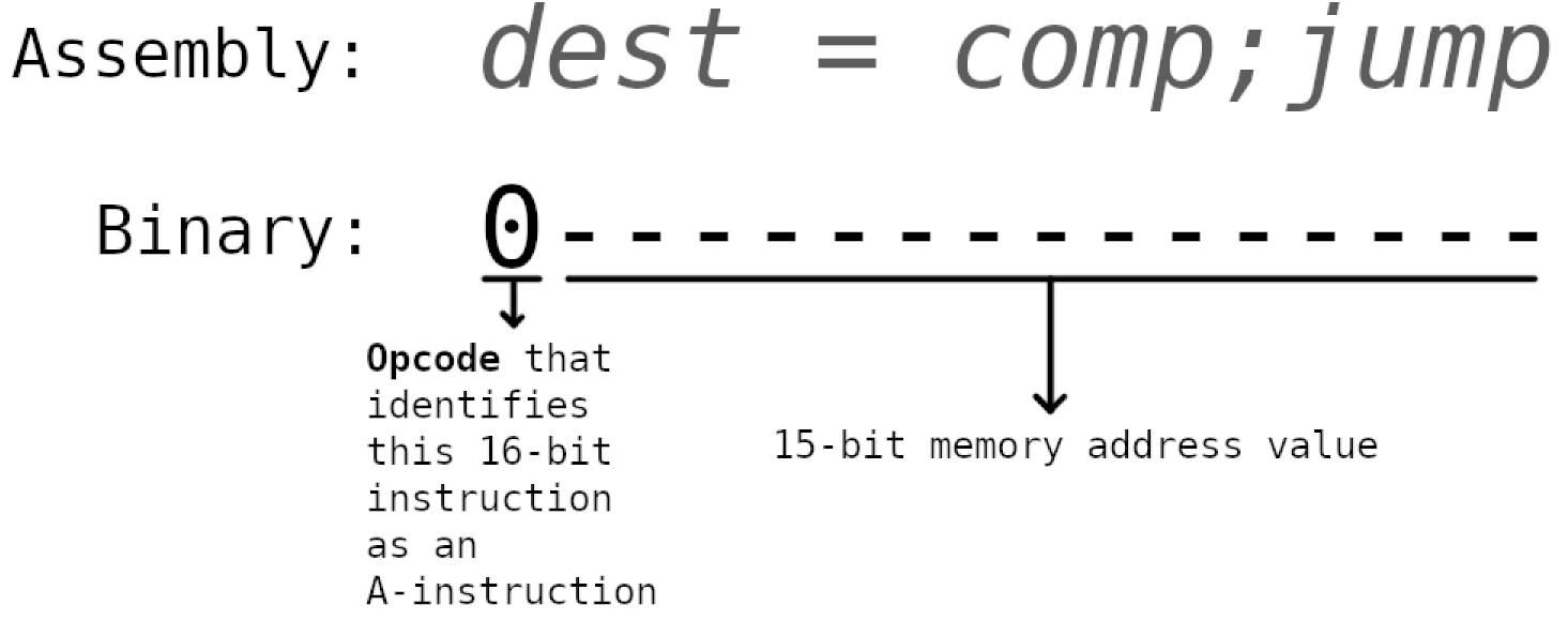
A-instruction structure. 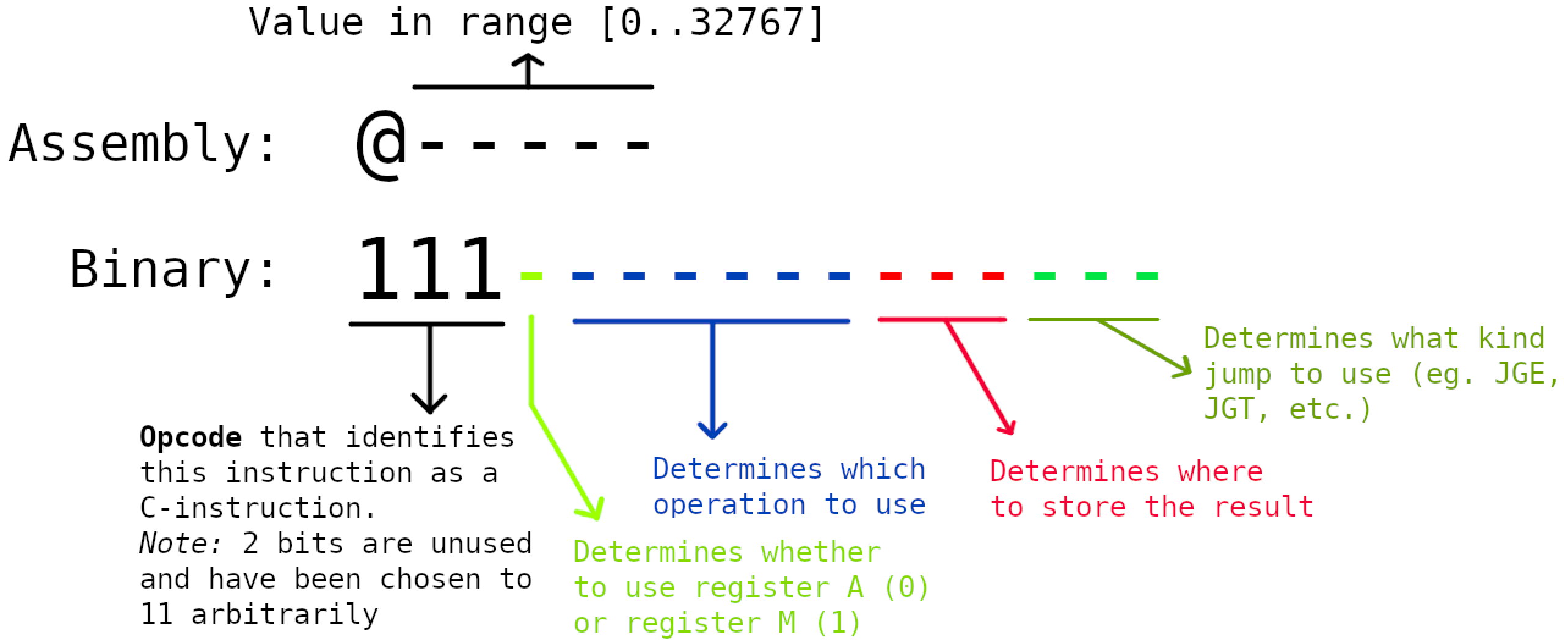
C-instruction structure. At this stage, we're only defining a standard and not building out anything. Once the standard is defined, we'll use it to guide the design of a CPU that can take in 16-bit instructions and execute them directly by routing each bit of the instruction through multiplexers, registers and the ALU to achieve what the specification defines.
-
Memory-mapped I/O for interfacing with peripherals and other I/O devices — there are a bunch of distinct types of I/O devices like mice, keyboard, microphones, speakers, etc. but the computer can interface with them all in the same way through a common abstraction called memory-mapped I/O. Basically, all I/O devices hooked up to the computer get a designated chunk of memory in RAM to store the data inputted to and outputted by the I/O device. In the Hack machine, we dedicate a chunk of the total address space to a screen (where each 16-bit register contains the on/off value of a pixel on the black-and-white screen), and a keyboard which only gets a single register that is meant to contain the code of whatever character is currently being pressed by the user.
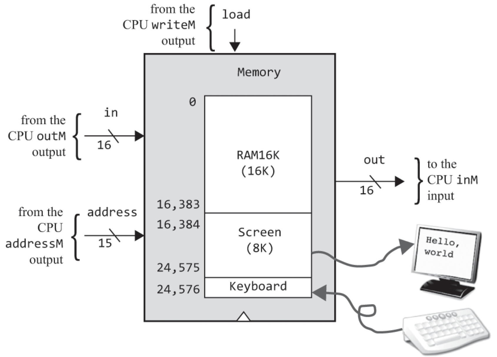
Memory-mapped I/O. -
CPU design and implementation — it's time to put everything together. The aim of the CPU design is to support the instruction set defined previously, enabling it to support general-purpose programmability. This can be achieved by using multiplexers to route the bits of a 16-bit instruction to the other chips aboard the CPU, namely the dedicated registers and ALU. The following minimal design is sufficient to support the instruction set.
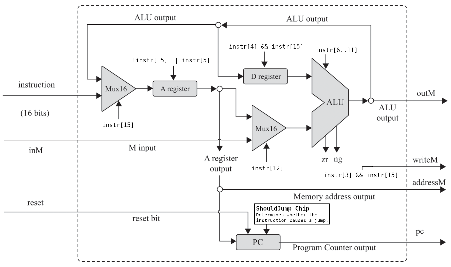
Hack CPU implementation. -
Fitting everything into the Von Neumann architecture to complete the general-purpose computer — With the CPU (plus the ALU) and RAM both implemented, we can compose them together according to the Von Neumann architecture below. This forms a complete general-purpose PC, which when booted up will fetch an initial instruction emitted from the ROM chip that directs the CPU to begin executing instructions for loading the OS kernel into main memory (this process called OS bootstrapping). When the user hits the reset button, it’ll cause the CPU to set which causes the first instruction in to be emitted and execution to start from the beginning again. In each clock cycle, the CPU accomplishes the entire fetch-decode execute cycle to fully execute one 16-bit instruction emitted from the data memory device.
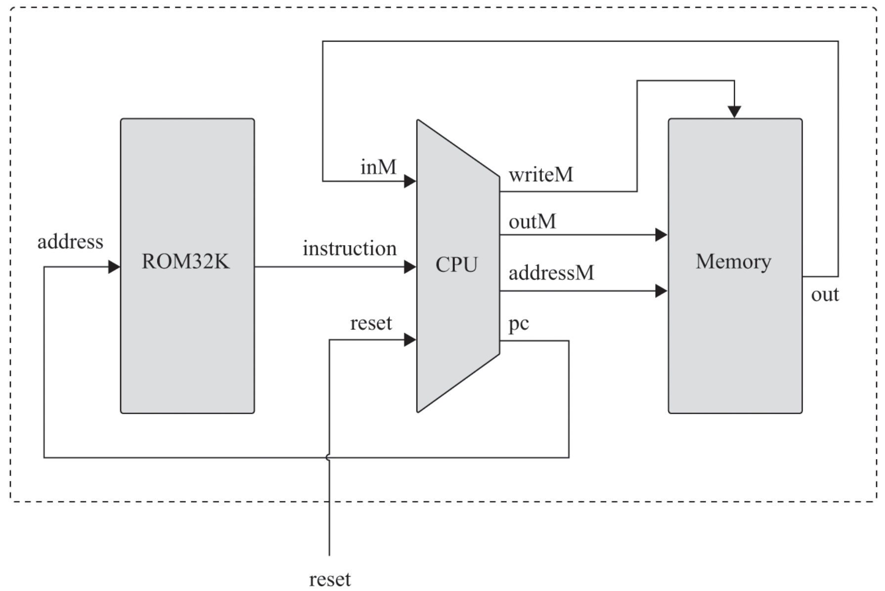
Hack computer assembled based on the Von Neumann architecture.
The difference between this simple 16-bit computer and modern personal computers is obviously massive. Notably, this computer is missing the dedicated graphics processing hardware and non-volatile storage devices that make computers more useful to people. Many of the complexities in modern computer arise from the profitable pursuit of optimisation and security. In this project, we only considered barebones functionality, but the remarkable thing is that this computer is capable of almost anything that modern modern computers can perform.
Hack Assembler
Assemblers are a special class of compilers that convert source code written in an assembly language into machine code that is directly executable by the CPU.
For this project, I wrote an assembler using C++ that converts code written in the Hack assembly language into machine code directly executable by the CPU.
See the GitHub repo.
Hack Assembler Usage
make                        # Compiles and produces the `HackAssembler` binary.
./HackAssembler <asm-file>  # Compiles the given .asm file to a .hack file, with
                            # each line containing the plaintext machine code.
Jack Virtual Machine & Compilation Model
See the Jack language specification and JACK VM language provided by Nand2Tetris (CSIE slides).
In the next two projects, I implemented a VM translator and compiler, each using C++, CMake and GoogleTest, which work to compile Jack source code based on a 2-tier compilation model that is similar to the standard compilation of high-level languages like Java and C#.
Jack is an LL(1) 'object-oriented' programming language. The Jack compilation model works in two stages, the first involves using the Jack compiler to generate Jack VM code, which can then be run by the Jack Virtual Machine. The Jack Virtual Machine is a stack-based virtual machine that relies on a VM translator to convert the Jack VM code into Hack assembly code.
This idea is inspired by Java's compilation model where a Java compiler converts Java source code to bytecode which can be executed by the Java Virtual Machine. The the VM code is then mapped to the hardware platform's assembly language, then finally converted to machine code by the assembler.
Jack VM Translator
The Jack VM translator is responsible for taking input written in the Jack Virtual Machine language (which is similar to Java bytecode) and mapping it to Hack assembly language. I implemented the VM translator using C++.
See the GitHub repo.
Jack VM Usage
The VM translator maps a given .vm file into a corresponding .hack file.
make                         # Build the `VMTranslator` binary
./VMTranslator <vm-file>     # Translates a single .vm file to an .asm file.
./VMTranslator <directory>   # Translates all .vm files in the given directory to a single merged .asm file. Assumes that the directory only contains .vm files that you intend to translate.
Jack Compiler
The Jack compiler, developed with C++, CMake and GoogleTest, is responsible for compiling files written in the Jack programming language into the Jack VM language, which can be passed to the Jack VM translator to ultimately obtain executable machine code.
See the GitHub repo.
Jack Compiler Usage
# Build and run.
cmake -S . -B build   # Generate the cross-platform build system (make sure to install CMake).
cmake --build build   # Build the compiler.

./build/JackCompiler <file>        # Translates a single .jack file.
./build/JackCompiler <directory>   # Translates all .jack files in the given directory.
By default, JackCompiler outputs VM code to files along the same path as the
input .jack source files.
To run tests for the compiler:
# Run unit tests.
cmake --build build
cd build && ctest --verbose   # The --verbose option outputs GoogleTest's test failure messages.

# Run integration tests.
sh SyntaxAnalysisTest.sh
sh CodeGenerationTest.sh

# ... or:
chmod +x SyntaxAnalysisTest.sh
chmod +x CodeGenerationTest.sh
./SyntaxAnalysisTest.sh
./CodeGenerationTest.sh
Hack OS
The operating system for the Hack machine is written in Jack. It's an incredibly rudimentary operating system which only implements a basic heap memory management algorithm, screen graphics drawing algorithm, keyboard I/O, math functions not implemented by the ALU aboard the CPU, and so on. See the GitHub repo.
That's pretty much all. It's absolutely nothing compared to the complexity and ecosystem of a mature, industry-strength operating system like Linux which implements filesystem abstractions, virtual memory, interrupts, syscalls, security mechanisms, multi-threaded and multi-process job scheduling, and so on.
Closing Note
Building out everything in this project taught me so much, from digital logic design to basic operating system development. I felt that a lot of what I learned in this project filled critical knowledge gaps that I failed to cover in my computer science education. For instance, I went through 4 years of university never knowing exactly how a CPU was able to just 'execute' machine code, or how Java code was able to be translated to platform-specific machine code. This project taught me all of that, and unveiled a lot of the black box magic hidden within this big hunk of metal, silicon and plastic that's running the software I'm typing this sentence into. I have a newfound appreciation for all the levels of abstraction put neatly in place by all the brilliant scientists and engineers, all for me to be able to write buggy javascript code.